
Welcome to
Azur Electronics
Azur Electronics
REPAIR HP 8657B
SIGNAL GENERATOR
SIGNAL GENERATOR
Home
Projects
Test Equipment
- Accessories
- Adaptors
- Amplifiers
- Attenuators
- Cables
- Frequency Counters
- Logic Analysers
- Multi-Meters
- Network Analysers
- Oscilloscopes
- Power Meters
- Power Supplies
- Prototyping Equipment
- Signal Generators
- Spectrum Analysers
- Tools
Operating Information
- Operating HP 141T
- Operating HP 1630D
- Operating HP 8175A
- Operating HP 8407A
- Operating HP 8410C
- Operating HP 8552B IF Section
- Operating HP 8553B RF Section
- Operating HP 8554B RF Section
- Operating HP 8555A RF Section
- Operating HP 8556A LF Section
- Operating HP 8594E Spectrum Analyser
- Operating HP 8901B
- Operating LeCroy 9310
Technical
- Allen Key Sizes
- High Voltage Measurement
- HP Cases
- HP Information
- HP-IB Interface Bus
- Measurement Units
- Motorola ECL
- RF Connectors
- RF Power - Voltage Conversion
For Sale
Wanted
Links
About Me
Contact Me
Site Map
July 2015
The HP 8657B Signal Generator on initial testing indicated a problem. Frequencies between 1100MHz and 1300MHz did not have an RF output and the overall output levels were not flat over the frequency range within ±1.0dBm.
The HP 8657B Signal Generator on initial testing indicated a problem. Frequencies between 1100MHz and 1300MHz did not have an RF output and the overall output levels were not flat over the frequency range within ±1.0dBm.
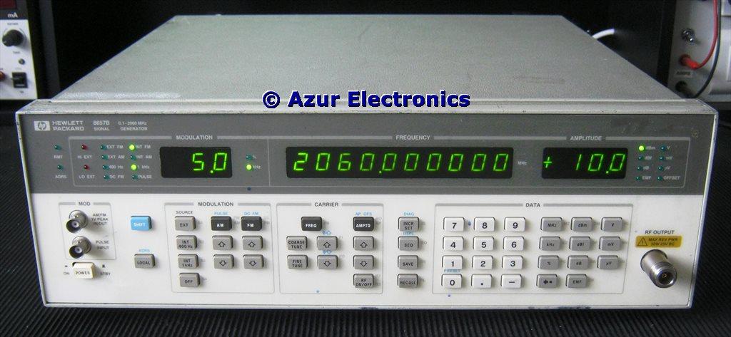
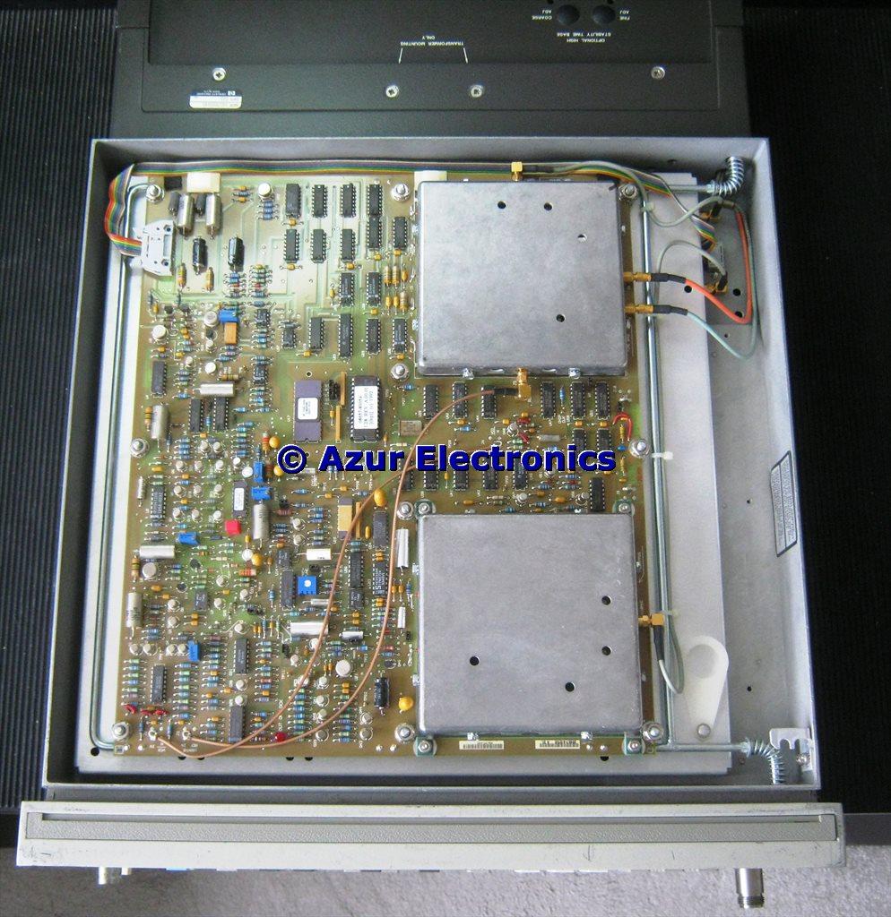
Front view
Decided to start with the Adjustments in the Operating and Calibrating Manual. Adjustment 1c checks the +5V, -5V, +15V, -15V & +38V power rails. All ok except -5V. This actually should be -5.2V ±0.02V but was low at -4.8V max.
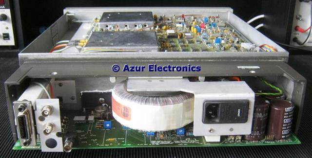
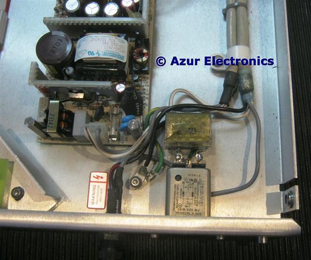
Removing the Rear Panel and Fan reveals the Power Supply PCB
The -5V Regulator U2 LM337 was faulty and could not supply any load current, so it was replaced. Voltage rails now all within specification. A previous repair had replaced the +5V rectifier CR6 but there was still some damage to tracks and to C18 & C19. The tracks were cleaned up and the capacitors replaced.
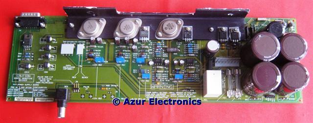
Power Supply A14 Assembly
The Heatsink was cleaned up and new thermal compound applied before re-assembling. The whole power supply circuit was tested to confirm correct operation.
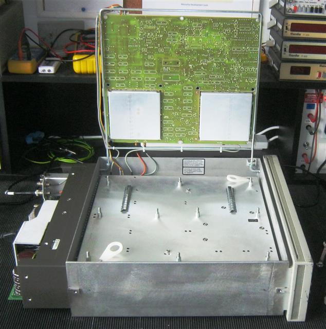
The Adjustments procedures requires access to various Assemblies which involves partially dismantling the 8657B.
The Adjustments procedures requires access to various Assemblies which involves partially dismantling the 8657B.
Power Supply A14 Assembly
The A11 Audio Board was removed and inspected, no obvious faults.
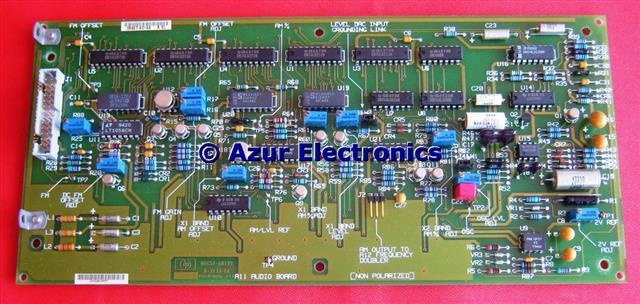
A11 Audio Board
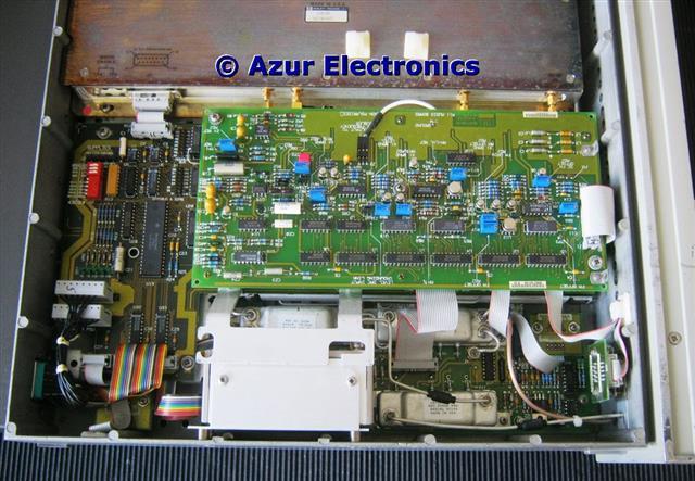
Underneath the A11 Audio Board is the A13 Processor Board.
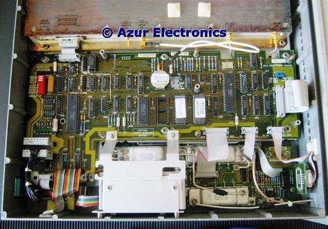
Bottom view showing A13 Processor Board
A13 was also removed and inspected, no obvious faults. The battery was checked ok at 3.22V. There is a wire link modification U3 SN74ALS133N pin 7 to U21 DM74LS14N pin 13.
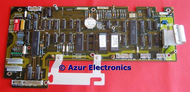
A13 Processor Board
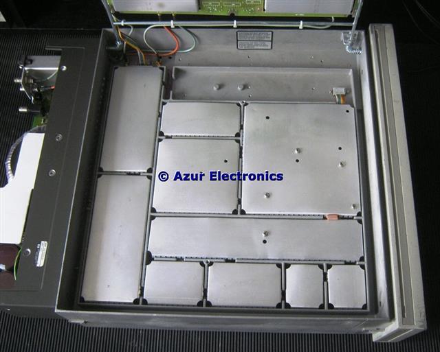
Bottom view showing A9 Attenuator, A10 Attenuator Drive
and A12 Frequency Doubler in Screened Box
and A12 Frequency Doubler in Screened Box
Underneath the A13 Processor Board is a RFI screen covering the A9 Attenuator and A10 Attenuator Drive Board. These will be much more difficult to get access to for maintenance. The A12 Frequency Doubler is in the screened box at the top.
Top view showing A3 LF Loop Board
A3 Board has the 50MHz Oscillator in a screened cover at the top and the LF VCO A3A1 in a screened cover at the bottom.
Top view showing A3 LF Loop Board and RFI Screened Cover
Unusually, the A3 Board hinges up to the right hand side and there is even a retaining clip to hold it in place. Underneath A3 is a RFI screened cover.
Top view showing individual RFI Screened Covers
Lifting the RFI screened cover off reveals more assemblies. Each of these has their own RFI screening.
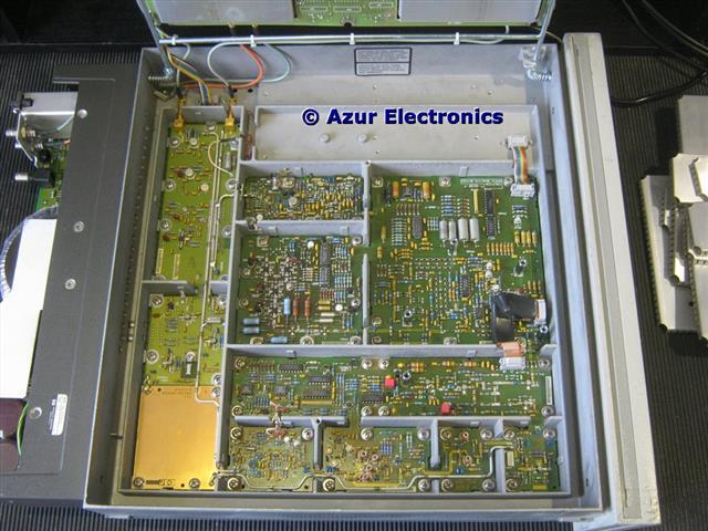
Top view showing individual RFI Screened Covers
These Assemblies are:
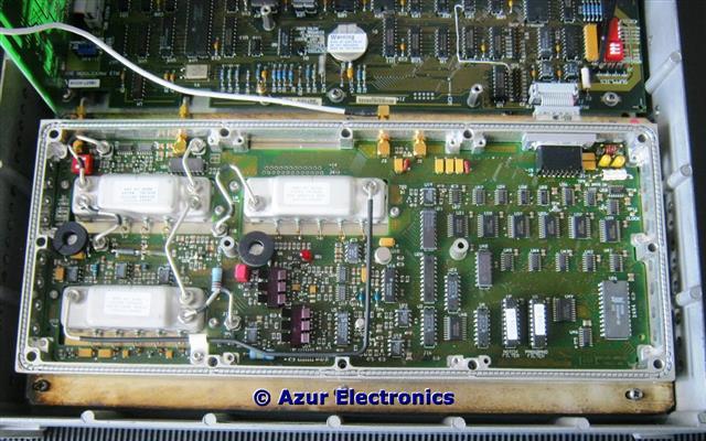
A8 Frequency Multiplier Assembly (Top Left 2 Sections) 08656-60221
FL1 Filter (Bottom Left 1 Section) 08656-60005
A6 Output Assembly (Top Right 3 Sections) 08657-60196
A4 HF Loop Assembly (Bottom Right 5 Sections) 08657-60102
Maintenance of these Assemblies will be difficult because of the rigid coax lines. It will probably need all of the PCB Assemblies being lifted out together, lots of screws and fragile connections!
Continuing with the Adjustments from the Operating and Calibration Manual.
1c. Power Supply - OK
2. Reference Voltage - OK
3. Audio Oscillator Level - OK
4. AM Offset - OK
5. 50MHz Reference Oscillator Level - OK
6. 50MHz Reference Oscillator Frequency - OK
7. 122MHz Harmonic - OK
8. 400MHz Bandpass Filter - I don't have a 8902A Measuring Receiver so used the 141T Spectrum Analyser instead. To connect to the A8 PCB a special adaptor probe is required 1250-1598, again I don't have one so made up an adaptor out of a spare N-type connector with rigid coax.
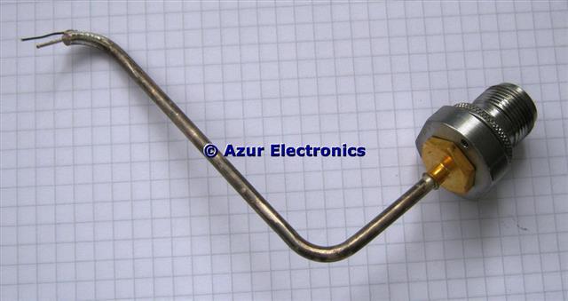
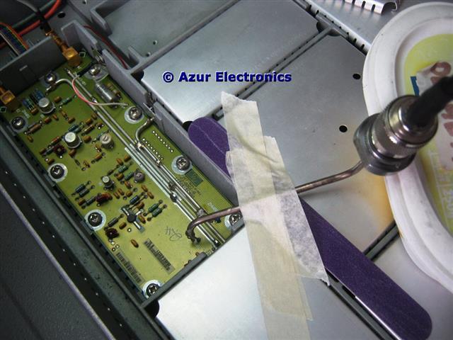
Alternative to 1250-1598 Adaptor Probe
Not pretty but it worked and you have to be very careful not to short out the output at TP3 on the A8 PCB. Tricky connection but adjustment OK.
9. 690 to 740MHz IF Compensation and Attenuation Pad Select.
Could not get a meaningful trace on the Spectrum Analyser.
10. Notch Filter - OK
11. 400MHz Notch Filter - OK
12d. Level and ALC Loop Detector.
Levels slightly low so out of spec.
13. AM% and ALC Loop AM - OK
14. AM% in the Double Band - OK
15. FM Calibration Pretune - OK
16. API 1,2,3 & 4.
Could not see any spurious signals at -60dB on the Spectrum Analyser.
17. Pedestal - as 16.
18. Integrator Input Offset - OK
19. DC FM Spurious Signal - as 16.
20. Voltage Offset - OK
21. DC FM Offset - OK
22. FM In-Band Gain - OK
23. FM Deviation - OK
24. 10MHz Reference Oscillator Frequency - Option 001 only.
After carrying out all the adjustments, the 8657B is now working at all frequencies 100kHz to 2060MHz except for no output in a narrow band at 1030 to 1039MHz. Checking the frequency response the output is fairly flat except 5dB approx. down at 500MHz and falling off below 750kHz. Checking the attenuator at various frequencies and there is a problem above +7dBm with low output.
So some improvement but still problems to resolve.
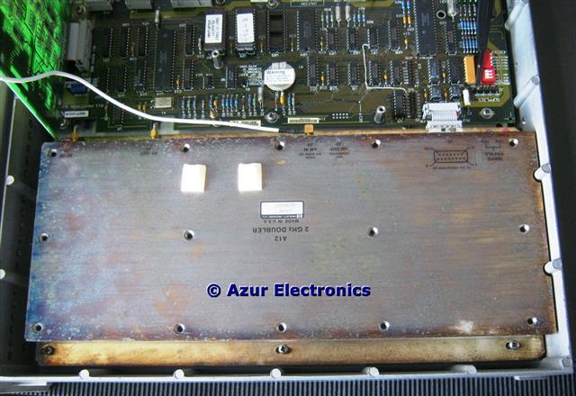
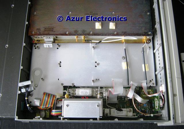
A12 2GHz Doubler
I have managed to work out the connections at J1 between A13 (08657-60206) and A12 (HP 11828A 3427A05857) both of which are different to the Service Manual. Essentially 8 power rails, 3 inputs, 3 outputs and ground on a 15W D connector. One of the inputs to A12 'X2 LAT' from A13 U5 pin 7 is being held at +4.5V by A12. Disconnecting A12 and there is 5V -ve going pulses when FREQ is incremented/decremented. The other 2 inputs 'X2 DA' & 'X2 CLK' look ok. 2 of the outputs from A12 'X2 DA IN' & 'X2 I(L)' are both held constant at around +4V. The other output 'X2 SH aka X2ANBUS' is at 0V up to 1039.999999Mhz and switches to +2V at 1040MHz and above.
A12 2GHz Doubler with cover removed
Unfortunately, I can't find a circuit for A12 anywhere and the PCB is mainly SMT. So probably end of this repair attempt unless someone has service information for A12 or another solution? See below!
August 2015
Completed all the 'Troubleshooting' tests in Block Diagrams 1 to 4 and all ok.
The 8657B is working apart from this narrow frequency range 1030-1039MHz and the A12 ALC circuit is obviously not working, so the output levels are out of spec. See below!
December 2015
The second HP 8657B Signal Generator with Option 003 Pulse Modulation and Option 022 GMSK Modulation had a reported fault with "smoking!".
0.3 GMSK Modulator with faulty suppression capacitor
In the 0.3 GMSK Modulator unit, the suppression capacitor was blown. This is for electromagnetic interference suppression across the mains line. This is a fairly common problem. They are rated at 275Vac which is probably fine in the USA with mains line voltages of 115Vac, in the UK 230Vac is more significant. My local line voltage is 254Vac, right on the upper limit! A new suppression capacitor has been fitted.
The Computer Products NFS40-7610 SMPS has been tested ok. I don't have the facilities to test the Modulator although it powers up ok.
The second 8657B Signal Generator completed its User Confidence and Adjustment Tests ok.
February 2016
The first 8657B still had some problems: now not working at frequencies above 1029.999999MHz which made me believe that the frequency doubler was not working; and low output on the attenuator settings.
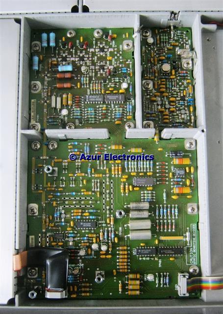
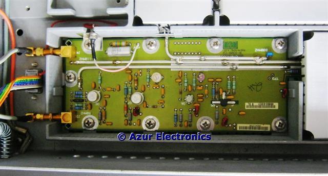
A6 Output Output Assembly
Checking levels all through the output circuitry identified a low output on A6. The fault was RF transistor A6 Q211, a MRF581 in the top left section, which also had the effect of disrupting the +7.5V supply to other parts of the circuit and disabling the frequency doubler. This was lucky as service information on the A12 2GHz Doubler is not available from HP.
The first 8657B is now working correctly. Completed all the User Confidence Tests (except HP-IB) ok.
The first 8657B is now working correctly. Completed all the User Confidence Tests (except HP-IB) ok.